The Design of a GPSDO - The Beginning
The Motivation
There is currently a discussion on the time-nuts mailinglis about designing a GPS Disciplined Oscillator (GPSDO). It is by far not the first discussion of this kind and most likely will not be the last. What makes this one stick out, though, is that that Tobias Plüss has put quite a bit of thought effort into the design and it shows. While a GPSDO is not the most difficult electronics a hobbyist or time-nut can build, it is one of those designs where the details matter a lot. A small short-cut taken here, a non-optimal component choice there and a lot of performance is suddenly gone. And it is not easy to see where the critical points are. As quite often when it comes to precision metrology, each and every step has to be carefully evaluated and judged on its merits and demerits.
If you read the above-mentioned discussion, you will notice that I pulled a GPSDO design of my own that I started way back in late spring/early summer 2017, to show where the important points are and how to get around some of the issues. During this discussion I realized that maybe, I should put all my design online, with a discussion what kind of thoughts and trade-offs went into it. I plan to post most parts of the design over the next couple of weeks, explaining the key points and what lead to the design choices I made. Some of these posts will be probably quite short, others will be quite long (I already dread the time it will take me to do a proper writeup of what went into the sine to square wave converter). So, stay tuned!
The History
I originally set out to do my own GPSDO because I was annoyed that easy features where generally not available in easily and cheaply available GPSDOs. The two main features I missed where having an ethernet port so that the GPSDO itself could act as an NTP or PTP server, instead of requiring a PC (or a single board computer) as an intermediary and to have multiple time-stamping inputs, potentially to be used together with additional references. The latter stems from the idea that we can realatively easily measure the frequency and phase difference between two local oscillators (or frequency sources, to be more general). Doing that, it would make sense to allow the use of an atomic frequency standard (think of a Rubidium vapor cell standard or a Caesium beam standard) act as mid-term reference. This way the local OCXO in the GPSDO would provide the short term performance (up to a few seconds), the atomic frequency standard would provide the performance up to several 1000 seconds and GPS would then be used to correct the drift in the frequency standard. So I set out to design a GPSDO with these features, but other than that, the design was pretty much what everyone else was doing as well.
You are probably asking yourself, if I had done this design 2 years ago, why is it the first time you hear of it. Well, there is the usual lack of time as an excuse, but the real reason lies elsewhere. In spring 2018, in one of our discussions, Tom van Baak wrote the following:
Another thought... For someone like you I think it would be better not to spend too much creative time to reproduce what was done in the 80's and 90's. Instead build a mostly digital GPSDO using a DDS. That avoids all the hassle of OCXO drift and tuning range and EFC and DAC and Vref; not to mention their combined tempco.
I have to agree here, Tom is right, we are not in the 1990s anymore. Today our the electronic components we have access to are amazing! They are low noise. They are cheap. They are easy to source even in low quantities. And you get amazingly good documentation. To top this off, we have more processing power in a small microcontroller than a PC had back then, at a fraction of the power consumption. So, using this input by Tom, did I adapt my design to the modern realities of today? Of course... not... My answer was quite dismissive:
As for using direct DDS based offset methods like in the FE-405 or Rick Karlquist's offset synthesizer. I had a look at those, but so far I couldn't come up with a scheme that do not require a lot of circuitry or gets restricted in the input frequency range.
Basically, I said using DDS based systems would be too complicated, in terms of electronics required, or too restricted in what they would allow to be worth the effort. The FE-405 design requires to design the whole system for one frequency only and it would not work if e.g. due
to aging, the oscillator deviated too much. If one wished to change the frequency, then the frequencies of the components would need to be redesigned, which makes the system hard to adapt to even quite benign changes (e.g. going from a 10MHz to a 12MHz OCXO). This was against my initial design requirements to have the system flexible enough to choose basically whatever OCXO was available. Of course with some trade-offs, when the frequency didn't fit the plan, but it should basically just work no matter whether it was an 10MHz OCXO or something odd like a 16.384MHz OCXO. And this is not yet touching the subject of the reference input and the local oscillator having a very specific difference frequency, which makes choosing the reference a pain. Additionally, the DDS spurs will be so close to the carrier that they will be hard to filter out (there is a reason the FE-405 has a crystal filter at the output). Similarly, Rick Karlquist's synthesizer (see his 1995 paper "A narrow band high-resolution synthesizer using a direct digital synthesizer followed by repeated dividing and mixing"), though it offers superb tuning fidelity (the DDS step size is divided down with every step, making it even finer than it is possible with the FE-405) and at the same time very low spurs (each division step reduces the DDS spurs), it has a very small tuning range (3 stages with 100kHz bandwidth filters result in about 400Hz tuning range) and a quite high circuit cost. And again, we are limited to a single frequency choice. But luckily it the reference can be, and has to be, arbitrarily close to the output frequency, which makes quite a bit easier than in the FE-405 style design. One could, of course, use a DDS directly to get the output frequency. But to produce 10MHz of output, one would need a DDS that runs at 100MHz or higher (using a DDS with an internal oscillator, for example). Of course, this would generate a lot of close in spurs, which are not what we want. Close in spurs can be reduced a lot by running the DDS at only integer multiples of the bit-width of the DDS core, which seems to be quite universally 19bit. But 19bit means we have only 190Hz frequency steps (at 100MHz clock frequency) while we want at least a resolution of one part in 10^-12 or 10µHz (at 10MHz). I.e. it is now a trade-off between spurs and resolution: The more bits we use to get higher resolution, the more and closer spurs we get. And we haven't touched the topic of refernce frequencies that are not 10MHz at all, yet. So neither of these approaches is quite what I was looking for. And that's why I dismissed Tom's comment so readily.
Of course, a mere three days after I wrote the above lines, I had an idea how to get around all this. A system that would retain the high resolution of a DDS while offering low spurs and allow to use a very wide range of reference frequencies. Unfortunately, the system would be so different from what I used to design that I need to put a lot of thought into it, to make the design deliver on its promises. Together with my lack of time, this made the whole project stall and thus has been sitting around half designed for quite some time now. There are still quite a few open questions I couldn't answer yet, so I do not feel comfortable to talk about it in greater detail, just yet.
The Overall Design
So, I will be talking about my "old" but ready design, to showcase the choices and decisions that went into it. Let us start with what my requirements were:
* I should be able to solder it by hand. So no components that require a reflow oven (like DFN, BGA, etc)
* Should accommodate different OCXOs so people can use whatever they have at hand
* Multiple time-stamping inputs. Either too be used to measure other devices or to use a more stable standard (i.e. an atomic frequency standard) as an additional reference for enhanced performance
* Powered from a standard, easily available power supply in the 12-24V range.
* The on-board power distribution should be efficient. I.e. no linear regulator that converts 24V down to 12V for the OCXO and consumes 12W constantly.
* Serial port with PPS output to be used with Lady Heather
* USB port (maybe with PPS output using Interrupt packets) to be used with Lady Heather
* A high resolution ADC for temperature measurement using PT100 or NTCs thermistors.
* Some additional ports and pins for extensions (e.g. a display)
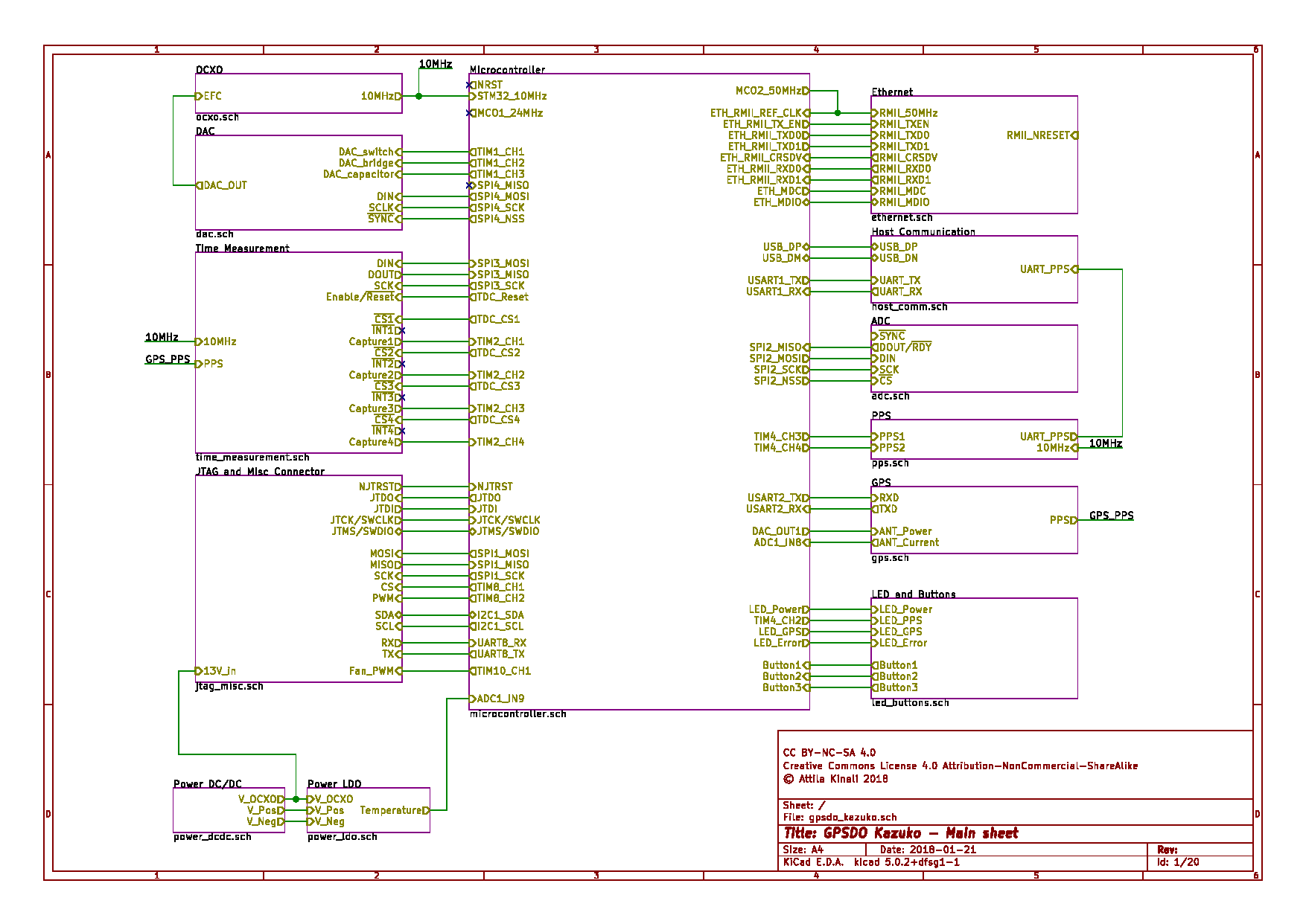 The overall design I came up with is pretty straight forward. There is a microcontroller that sits in the center and controls all the other components. On the right side of the schematics, you see the OCXO block, including a sine to square wave converter, so the rest of the circuitry has proper CMOS signals. The time-stamping block, which is used both, to time-stamp the PPS from the GPS receiver to discipline the OCXO, as well as external signal sources. There is an ethernet block, an host communication block with the serial and USB interfaces. The ADC for the thermistors. A block to correctly form low jitter PPS output pulses. Of course the GPS receiver deserves its own block. And there is one block with LEDs and buttons, because who wouldn't include some Blinkenlights in a project like this. Wedged in the left bottom corner, are two blocks that make up the power supply, which is split into a block with switched DC/DC converters and one with LDOs to ensure high efficiency, while not being so noisy as to degrade the performance of the system.
While most of this is unsurprising, there are a two points I would like to draw your attention to. These are the time-stamping and the frequency generation for ethernet and USB.
Starting with the frequency generation, USB requires a 48MHz clock. As with most modern microcontrollers the USB core is completely embedded in the microcontroller itself including its clock generator PLL. No surprises there. Ethernet on the other hand, is split into a part that is included in the microcontroller (the MAC) and a part that is external (the PHY). The PHY needs an clock of 25MHz or 50MHz depending on whether it uses standard MII (media independent interface) or RMII (reduced media independent interface). I didn't want to include another crystal oscillator, especially one that runs unlocked to the OCXO. But adding another PLL just for the crystal was a bit much. Luckily, the microcontroler I chose, an STM32F427, has pins which can output the internal clock, one of them even at 50MHz. So I use the microcontroller's internal PLL to generate the ethernet clock. It's not the lowest noise clock source, but it should be good enough for this application. There is a second such clock output pin that can be used, which I designated as 24MHz clock, in case I wanted using a USB HS, which requires an external ULDPI interface chip. In the later design stages it became clear that this was not going to happen, as I already used up most of the pins and couldn't free up the USB HS interface. But using a variant with larger package and more pins would make it theoretically possible. Hence the pin is still there, but not connected.
The time-stamping is made slightly weird when you look at it at first. As you can see, there is a "Capture" signal going to the microcontroller and it ends up at timer inputs. Time-stamping or rather time-to-digital converters usually operate as a two stage process. There is a fine counter, that measures the event time precisely and there is a coarse counter that provides the long term measurement. Kind of like having a watch and a calendar. The watch tells you when in the day something happend and the calendar which day it was. The reason for this split is the difficulty of making long time measurements precisely. Like with the watch and the calendar analogy, if the watch has to run for days or weeks, it will go slightly off. But if you reset it every day at midnight, you will have an accurate clock throughout the day.
The general idea how the time-stamping should work was taken from John Ackermann's TICC design. But I wanted to further simplify it. So instead of using a divider to make the fine measurement period long enough that the Arduino, he used, could capture the event, I chose to use the capabilities of the much stronger STM32F427, which includes a fast timer unit. So instead I use a very short measurement period and let the timer unit of the microcontroller act as a coarse counter. More on this on a later installment, when we cover this block. Design wise, I could have simplified it further by using an FPGA to handle the TDCs and implement the coarse counter there. Particularly as this would allow an almost unlimited number of time-stamping inputs. But I shied away from adding another programmable device as this is another piece that would need to be correctly programmed for the whole system to work. Especially as an FPGA, unlike a microcontroller, has relatively poor debugging capabilities. So unless I really had to use an FPGA, I did not want to have it in there.
Ok, this has gotten a lot longer than I intended it to be for an introduction. I will looking at the details of the first block for next time.
- Attila Kinali's blog
- Log in to post comments